
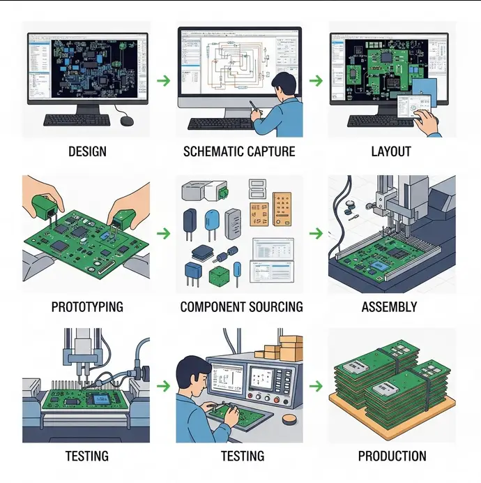
Understanding PCB Design Fundamentals
A successful electronics project starts long before any schematic is drawn or PCB is fabricated. The process begins with clear requirements and a well-thought-out design strategy that anticipates future needs, manufacturing challenges, and quality standards.Setting Clear Requirements and Specifications
Thorough requirements definition lays the groundwork for every successful PCB design. Before launching into design, consider:- Functional specifications (digital/analog circuits, sensors, interfaces)
- Electrical constraints (voltage, current, power consumption)
- Environmental factors (temperature, humidity, mechanical stress)
- Size and form factor restrictions based on product housing
- Regulatory standards (CE, FCC, RoHS) applicable to the final product
Creating the System Architecture
Good system architecture clarifies circuit organization and subsystem interaction. During this phase, select core components (microcontrollers, analog chips, wireless modules) and settle on key electrical and mechanical interfaces. Tools like block diagrams help visualize connections and guide schematic creation, while simulation software predicts performance before real-world testing. Collaboration between electronics and mechanical teams ensures the PCB fits seamlessly within the product enclosure (mechanical services). Design choices here affect manufacturability, serviceability, and compliance.Schematic Design and Component Selection
With a solid foundation, attention shifts to detailed circuit design and component selection. This phase translates the architecture into an actionable electronic blueprint.Schematic Capture
Using modern CAD tools (Altium, Eagle, KiCAD), engineers map electronic logic and signal flow. Proper documentation and naming conventions simplify review and modification. Attention to detail is critical:- Clear labeling of power rails and signal nets
- Correct part numbers referencing verified datasheets
- Inclusion of decoupling capacitors, pull-ups, and protection components
Selecting the Right Components
Choosing components affects not only functionality, but also longevity, cost, and supply chain stability. Consider:- Availability from multiple vendors to avoid single-source risk
- Lifecycle status (avoid obsolete parts)
- Thermal and electrical ratings within design margins
- Mechanical compatibility with PCB footprint and enclosure
PCB Layout and Design for Manufacturability
The transition from schematic to PCB layout blends engineering skill and aesthetic sensibility with real-world manufacturing expertise.PCB Layout Best Practices
Placing and routing components is part science, part art. Key layout principles include:- Separate high-frequency and low-frequency circuits to minimize interference
- Keep power and ground traces wide and minimize loop areas
- Avoid sharp trace angles and maintain consistent trace width
- Place connectors and mounting holes according to enclosure constraints
- Use ground planes to combat EMI and ensure signal integrity
Design for Manufacturability (DFM)
DFM ensures the PCB is easy and cost-effective to manufacture. Prioritize:- Standardized component footprints and pad sizes
- Sufficient spacing between pads and traces for soldering
- Inclusion of test points for in-circuit testing and debugging
- Avoidance of unnecessary complexity in board shape or layers
Prototype Fabrication and Testing
Once the PCB layout is finished and verified, move to prototype fabrication and hands-on testing to validate the design.PCB Fabrication
Send production files (Gerber, BOM, pick-and-place) to a reputable PCB manufacturer. For initial prototypes, fast turnaround services enable quick feedback. Review stencils, silkscreen labeling, and solder mask for clarity and ease of assembly.Assembly and Testing
Our in-house assembly expertise at Nuts and Boltz enables both manual and automated soldering, plus focused inspection for component placement and solder joints (gallery of projects). Key tests include:- Power-on and smoke tests for initial safety
- Functional tests for each subsystem (microcontroller startup, sensor response, wireless connectivity)
- Verification of key electrical parameters with oscilloscopes, multimeters, and logic analyzers
Refinement and Quality Assurance
Success hinges on refining the prototype into a production-ready design. This phase focuses on robustness, compliance, and repeatability.Environmental and Stress Testing
Expose prototypes to real-world conditions matching their intended environment:- Thermal cycling between operating extremes
- Vibration and shock testing for portable or automotive devices
- Humidity exposure, especially for devices in outdoor or industrial use
Final Design Validation
Collect user feedback, simulate mass production process, and finalize all bill of materials (BOM) and documentation. Update manufacturing data to reflect any layout or component changes. A robust validation process sets the stage for sustainable production.Preparing for Volume Production
Scaling up for manufacturing calls for strategic planning in supply chain management, quality control, and logistics.Supply Chain Optimization
Work with suppliers to forecast demand and establish flexible procurement channels. Secure backup vendors for critical or custom components to avoid supply disruptions. Nuts and Boltz provides direct support in vendor management and production scheduling for efficient volume ramp-up (track your order).Quality Control Procedures
Implement automated optical inspection (AOI), in-circuit testing (ICT), and statistical process control (SPC) at every stage of manufacturing. Maintain traceability through serial numbers or barcodes for every board produced. A consistent quality assurance system minimizes defects and warranty costs while enhancing customer confidence.Common Pitfalls and Troubleshooting
Even experienced teams run into PCB challenges. Awareness and preventive action help avoid problems:- Signal Integrity Issues: Use ground planes and correct trace routing to prevent noise and voltage fluctuations.
- Thermal Management: Provide heat sinks, ventilation, or thermal vias for high-power components.
- Component Obsolescence: Confirm that all components are in active production and have second-source options.
- Testability: Add extra test points and design for easy debugging.
Real-World Case Studies
Explore how our clients have succeeded across industries by leveraging our end-to-end PCB development services (portfolio):- IoT sensor platforms for smart cities with robust environmental protection and RF optimization
- Industrial control units for factory automation with high EMI resilience and advanced diagnostics
- Medical device prototypes with miniaturized layouts, biocompatible enclosures and compliance testing
